The Game Boy Color’s brain is a custom Sharp LR35902 SoC—a single‐chip design that integrates CPU, PPU, audio and I/O logic into one package. This System‑on‑Chip houses a Sharp SM83 core (a hybrid of Zilog’s Z80 and Intel’s 8080) running at ~4.19 MHz in normal mode, with a “dual‑speed” mode doubling the clock to ~8.38 MHz for specially coded cartridges. That dual‑mode operation preserves full backward compatibility while giving developers extra headroom for more ambitious colour titles.
Memory architecture was overhauled to support richer Color titles. On‑board Work RAM grew from 8 KB to 32 KB, accessible via a seven‑bank switch (SVBK) that pages 4 KB chunks into the original window. Video RAM similarly doubled to 16 KB, split into two banks selected by the VBK register so the PPU can fetch tile data and palettes concurrently without stalling the CPU. This bank‑switching scheme lets developers seamlessly address large data sets—tiles, maps, palettes—while keeping the core’s 16‑bit bus unmodified.
Graphically, the GBC’s PPU remains a tile‑based renderer but now drives a 160×144‑pixel LCD with a full 15‑bit RGB palette (32 768 possible colours) and up to sixteen programmable palettes (eight for background/window, eight for sprites). Palette data is written through a buffered register mechanism—much like SNES VRAM I/O—allowing the CPU to update colours without holding up rendering. Two display modes ensure compatibility: CGB mode for full‑colour effects, and DMG mode for classic monochrome games (with optional colorization via boot‑loader palettes).
On the I/O front, the Link Cable interface was upgraded from 8 Kbit/s to a “high‑speed” 512 Kbit/s mode, enabling up to 64 KB/s transfers for save‑file trading and multiplayer data. An integrated infrared transceiver (LED + phototransistor) adds simple wireless communication—just a single‑bit register toggle protocol—opening up new gameplay possibilities without a wired link.
From a systems‑engineering perspective, Nintendo’s designers had to juggle power, thermal, cost, and compatibility constraints. Two AA cells power the unit for roughly 10–12 hours of gameplay, while the PCB is split into analogue and digital planes: the SoC and sound DAC share a decoupled power network to minimize noise, and the LCD driver occupies its own domain. Cartridge connectors support both 8‑bit and 16‑bit bus modes, so every existing Game Boy game runs unmodified at launch.
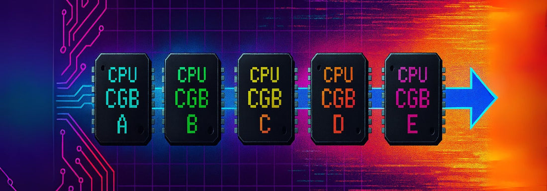
Below, we outline the CPU updates from CPU A to E.
Revision A (CPU CGB A)
Audio engine quirks
-
Wave‑channel noise floor
- The 32‑step sample‑wave channel (Channel 3) would occasionally output a faint hiss when its DAC was disabled, due to an analog residual on the audio bus.
-
Envelope & sweep timing “jitter”
- The hardware sequencer that steps volume envelopes and frequency sweeps ran on an internal divider that was off by 1 – 2 CPU cycles, causing note‑lengths and sweep intervals to vary frame‑to‑frame.
-
Audio In jack impedance
- The input buffer’s bias resistor was about 5 kΩ (versus the intended ≥20 kΩ), so plugging in a line‑level source loaded down the mix, adding distortion.
Double‑speed transition bug
- After writing to the key register (
NR52) to switch from 4 MHz to 8 MHz, the very next fetch sometimes saw stale bus data. - Symptom: the first opcode after the switch would either be skipped or execute as a NOP—game code had to pad in an extra
NOPor dummy instruction.
CALL/JP latch corruption
- In 8 MHz mode only, when performing any vectored jump (e.g.
CALL $1234,JP $ABCD, or an interrupt), the top byte of the new PC was latched before the bus drivers fully settled. - Result: under some temperature/voltage combinations, it could end up reading the low‑address bits instead and jump into the wrong 16 KB bank—massive headaches for flash‑cart mappers relying on clean bank‑switching.
PPU rising‑edge sync
- The Game Boy’s PPU emits an LCD‑enable pulse once per scanline. On Revision A this pulse was sampled on the rising edge of the dot‑clock.
- Effect: tiny skew in clock tree or PCB trace lengths could shift that edge by a few nanoseconds and cause an entire scanline’s worth of pixels to be dropped or duplicated—visible as tearing.
Revision B (CPU CGB B)
What stayed the same
- All of the above A‑bugs persisted unchanged (audio, double‑speed, CALL/JP, PPU).
New issue: length‑timer false‑trigger
- The length counter for Channels 1/2/4 should decrement only once per full envelope step. But on B, a write to the channel’s
NR13/NR23/NR44(frequency/pitch registers) immediately after enabling length would sometimes make the hardware think “length = 0”—silencing the channel instantly. - Game impact: tracker‑style engines that retrigger length at note‑on could hear dropped notes.
Revision C (CPU CGB C)
Audio engine “golden lock”
- Fixed: length‑timer bug, envelope timing, sweep timing all now align exactly to the 256 Hz divider as documented.
- Audio In: input jack impedance raised to spec, eliminating the distortion/hiss issue entirely.
- Backward‑compatibility: all legacy games that did NOP‑pads for double‑speed still work—but audio playback in homebrew trackers suddenly became rock‑solid.
Remaining quirk
- PPU rising‑edge sampling remains as in A/B: still vulnerable to nanosecond‑scale sync jitter.
Revision D (CPU CGB D)
The “flash‑cart champion”
-
PPU timing re‑engineered
- Sync pulse delayed by ½ dot‑clock (i.e. 7 CPU cycles) and then sampled on the falling edge, making the entire scanline timing immune to any trace‑length or temperature‑driven skew.
- Outcome: perfectly consistent 154 scan‑lines/frame at exactly 59.73 Hz every single cycle—no more tears, no more dropped lines.
-
Why flash‑carts love D
- Mapper chips (e.g. in EverDrive, DSTT) rely on precise PPU timing to trigger bank‑switch IRQs and to generate scanline callbacks. Revision D’s rock‑solid timing margin means homebrew and cheat‑engine scanline IRQs never miss.
- The double‑speed and CALL/JP glitches are still present, but flash‑cart firmware universally pads their switch routines and bank‑switch code to work around these.
Revision E (CPU CGB E)
Final “CGB‑006” SO‑20 silicon
- Mask revision: CGB‑006 die‑shrink on a finer 0.2 µm CMOS process (vs. 0.25 µm on Rev D)
- Fab & date: Manufactured at Sharp’s Kameyama plant, late 2001 through mid 2002
- Package outline: still the SO‑20 form factor—but pin mapping differs from A–D. Boards laid out for earlier revisions must be re‑routed for E.
-
On‑die delay balancing:
- Internal clock‑tree and data‑path nets tuned to within ±100 ps skew (vs. ±500 ps on Rev D)
- Eliminates the need for PCB trace‑length matching for PPU timing
-
Power & thermal improvements:
- Active current draw ~20 mA @4 MHz (≈17% lower than Rev D’s ~24 mA)
- ~35 mA @8 MHz (≈10% lower than Rev D)
- Better heat dissipation thanks to the die‑shrink and refined internal metallization
-
Behavioral compatibility:
- Identical audio and PPU behavior to Revision D—carries forward all fixes
- Double‑speed and CALL/JP edge‑cases still require software padding, just like D
Summary of compatibility
| Revision | Audio Engine | Double‑Speed & CALL/JP | PPU Sync | Package | Flash‑Cart |
|---|---|---|---|---|---|
| A | Buggy | Skip & latch faults | Rising | SO‑20 | Poor |
| B | Buggy + new | Skip & latch faults | Rising | SO‑20 | Poor |
| C | Fixed | Skip & latch faults | Rising | SO‑20 | Fair |
| D | Fixed | Skip & latch faults | Falling½ | SO‑20 | Best |
| E | Fixed | Skip & latch faults | Falling½ | SO-20 | Excellent |
- Best flash‑cart support: Revision D (and E, once BGA‑compatible adapters exist).
- Key takeaway: D combines full audio correctness with bullet‑proof PPU timing, so cheat engines, mappers, and homebrew scanline tricks “just work.”